 ©Moritz Brehm
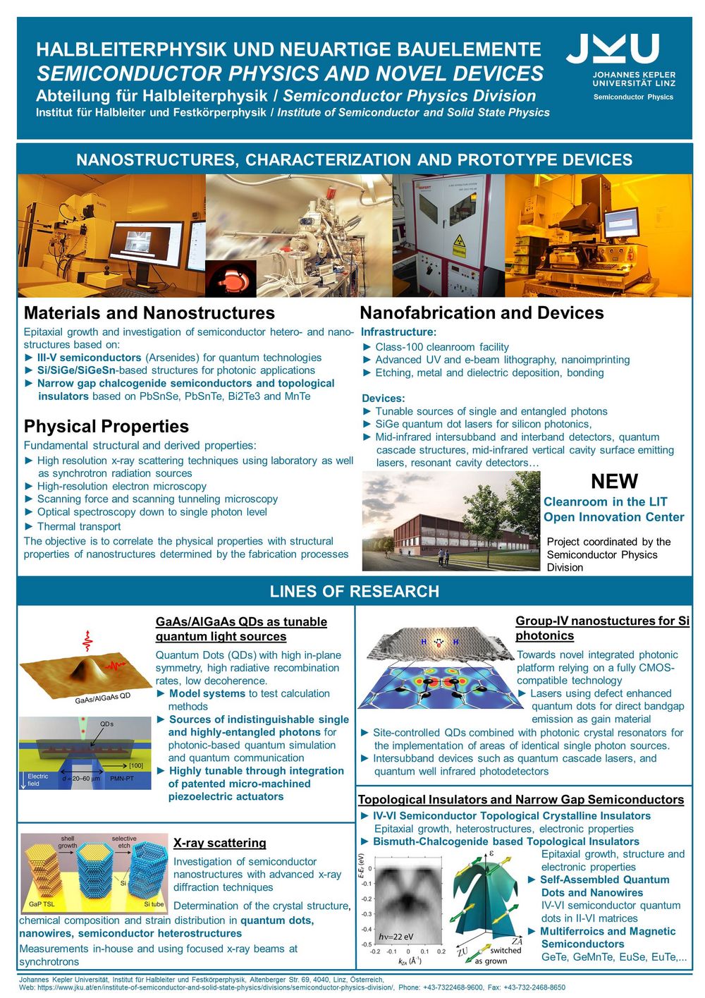
Research at the Semiconductor Physics Division is focused on the investigation and fabrication of semiconductor hetero- and nanostructures, ranging from nanofabrication, fundamental investigations and modeling of physical properties up to the realization of novel nanostructure devices for spintronic and infrared optoelectronic applications. Nanostructures are fabricated using advanced lithography and processing techniques including electron beam lithography, holographic lithography, as well as self-assembled growth of quantum dots using molecular beam epitaxy. For these purposes, a class 100 clean room facility with all necessary processing equipment is run at the institute. The objective of nanofabrication is to produce defect-free structures in the sub 50 nm range with good control of shapes and compositions, sharp heterointerfaces and excellent optical and electronic properties. A particular emphasis lies on the development of site-control techniques for positioning of self-assembled nanostructures.
The fundamental structural, electronic, optical and magnetic properties of nanostructures are studied using a wide range of techniques: from advanced x-ray scattering techniques using advanced laboratory as well as synchrotron radiation sources, high-resolution electron microscopy, scanning force and scanning tunneling microscopy, to optical spectroscopy as well as low temperature magnetotransport investigations. An important research goal is to correlate the actual electronic properties of nanostructures with the structural properties determined by the fabrication processes, taking advantage of the complementary information gained by the wide range of techniques and modeling tools. A strong emphasis is on infrared spectroscopy of interband and intersubband electronic transitions in SiGe and narrow band gap semiconductors heterostructures, as well as on ballistic and quantum transport studies of SiGe and III-V hetero- and nanostructures in the milli-Kelvin temperature regime. In addition, the magnetic properties of magnetic semiconductor hetero- and nanostructures are investigated, and novel tools for nanostructure investigations based on synchrotron light sources are developed.
Several research projects are devoted to the fabrication of hetero- and nanostructure devices, for mid-infrared intersubband and interband detectors, quantum cascade structures, mid-infrared vertical cavity surface emitting lasers, resonant cavity detectors as well as transport devices such as quantum dot and single electron transistors. In addition, novel spintronic devices are developed that exploit the spin degree of freedom for new functionalities.
From the materials side, a strong focus is on Si/SiGe based hetero- and nanostructures for which a molecular beam epitaxy system is operated in the clean room of the institute as well as another system devoted to in situ growth studies using scanning tunneling microscopy. The second major material system encompasses the narrow gap IV-VI compounds, based on PbSe and PbTe as well as the magnetic europium chalcogenide semiconductors. For these materials another two molecular beam epitaxy systems are operated at the institute. The fabricated samples and structures are also supplied to research groups outside of the institute in the framework of long-term international collaborations. Vice versa, also materials and structures from outside groups are investigated with techniques developed at our institute.
Johannes Kepler University Linz
Altenberger Straße 69
4040 Linz, Austria
 Go to JKU Homepage
