Quantum dots, i.e., small "islands" of a different semiconductor embedded in a crystalline matrix, are a main research focus of our group since several years. Many samples are produced at our institute in the SiGe MBE group and the IV-VI MBE group, but we also investigate samples in collaborations with international partners. In III-V compound semiconductors quantum dots are used to confine carriers and produce quasi-zerodimensional objects, e.g. InAs QDs in GaAs matrix. In light emitting devices such as lasers, the enhanced density of states can be used to reduce lasing thresholds, size and composition are parameters allowing to influence the emission wavelength. In the SiGe system, concepts to use the carrier confinement to overcome the indirect band gap and use Ge QDs in Si for optical emitters were not successful so far, but detectors based on SiGe QDs have been developed.
We have focused on the SiGe system, because it is an ideal model system concerning the growth mode of QDs (strictly speaking, most SiGe islands are too large to produce considerable lateral carrier confinement, and the term "quantum dot" therefore does not apply in all cases; we will not consider these differences here). When Ge is deposited on Si, in many cases using molecular beam epitaxy, first a 2D layer, the so-called wetting layer forms, which adopts the substrate lattice parameter in the growth plane and is therefore strained due to the 4.2% lattice parameter mismatch between Ge and Si. After a certain critical thickness of few monolayers, 3D islands spontaneously form, relieving part of the elastic strain at the expense of an increased surface. This relaxation mechanism is, however, not the only possible one. In almost any case, additionally intermixing between Si from the substrate and the deposited Ge occurs, resulting in a rather complex Ge distribution inside the islands, accompanied by a rather complex strain distribution. The details depend sensitively on the growth conditions. As a function of island size and chemical composition, a variety of shapes with different surface facets may form: pyramid-shaped islands are rather shallow, dome-shaped ones allow for more elastic relaxation due to larger aspect ratio, which is even bigger in barn-shaped islands.
Recently, SiGe islands have attracted attention due to their strain state: Elastic relaxation can be rather high in uncapped islands, if they are capped with Si, they exert tensile strain onto the cap. Since such biaxial strain lifts the valley degeneracy of the valence and conduction band, structures can be designed where carriers with a lower effective mass, and hence higher mobility carry the current. Compared to other methods to introduce strain into Si-based electronic devices, SiGe islands allow to reach higher strain values, without introducing lattice defects.
structural characterization
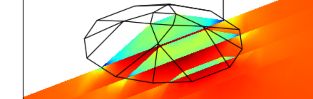
Our research focuses on the determination of the chemical composition distribution inside of quantum dots, and the strain distribution inside the dots and in the surrounding matrix and cap layers. For this purpose we record the intensity distribution around several Bragg reflections, to get information about the lattice parameter distribution. To analyze the data, model calculations are carried out, where the shape - often known from other techniques like AFM or STM - and the chemical composition distribution are refined until the simulations and experimental data match. To simulate the x-ray scattering, we first use a commercial finite element simulation package to calculate the strain distribution within the model, from which the diffraction pattern is calculated. As a result, we determined the evolution of intermixing for various growth conditions of islands, and the according strain distributions. This information can then be used by the optics group to calculate the electronic levels and resulting optical properties of the quantum dots.
Recently, we also use focused x-ray radiation to investigate single quantum dots, rather than ensembles of several 1000 to several millions of islands. This enabled, e.g., to study one single island embedded into a - fully functional - field effect transistor, where the channel is located in the tensile strained Si cap above the island. X-ray diffraction in this case offers the possibility to investigate the strain state of the completed device, with all metallizations etc. in place, without destroying it.
Johannes Kepler University Linz
Altenberger Straße 69
4040 Linz, Austria
 Go to JKU Homepage
