Located in the basement of the LIT Open Innovation Center and funded by the Austrian Federal Ministry of Education, Science & Research (BMBWF) in the frame of the HRSM project Center for Nanomaterials Research and Prototyping (CNP, in collaboration with the TU Vienna, Univ. Innsbruck, ISTA and FH Vorarlberg), the JKU and the state of Upper Austria, the new cleanroom has been designed for manufacturing scientific samples for fundamental research as well as producing prototypes to be shared with different institutes and departments (physics, chemistry, mechatronics, computer science), and with external collaboration partners and users.
Areas of application include quantum technologies, particularly new semiconductor-based light sources to secure data transfer via quantum key distribution, silicon-based photonics with potential applications in data transfer (data-centers), sensor technology, wearable electronics (e.g. for medical applications), ultra-light photovoltaics, etc.
The cleanroom environment drastically reduces the number of airborne particles and is vital to creating devices in the micrometer and nanometer range.
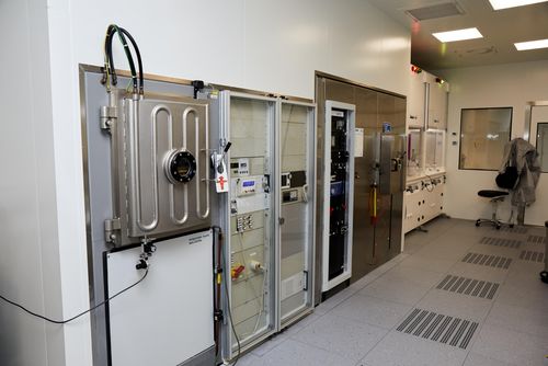
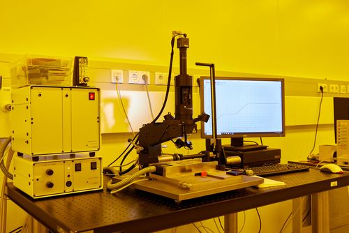
The cleanroom infrastructure covers the following areas with corresponding instruments:
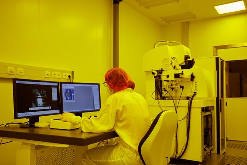
The Raith e-Line Plus is a system for the fabrication of nanostructures through electron-beam lithography. Electron-beam lithography (30 kV acceleration voltage) can be performed on substrates with sizes up to 4 inches (100 mm) in diameter. The laser stage with 10 nm accuracy is used to define micro- and nanostructures with typical sizes down to a few tens of nanometers.
Contact person: Armando Rastelli
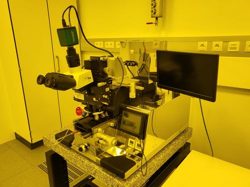
The Süss MJB4 is an optical lithography system for laboratories and small-volume production for substrate sizes up to 100 mm. High precision mask alignment and high-resolution printing capability are possible in the submicron range (0.5 µm). Additionally, one can perform a fast and accurate alignment with a single-field or split-field microscope. The Süss MJB4 is widely used for MEMS and optoelectronics applications.
Contact person: Thomas Fromherz
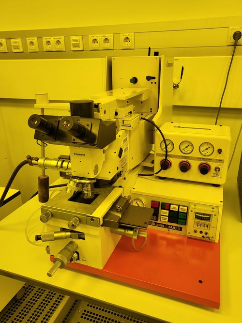
The Süss MJB3 is a standard Mask Aligner that can be used in a hard-contact-, soft-contact-, or vacuum-contact mode. For exposing substrates (sizes <3 inches in diameter), an arc-lamp with a wavelength of 365 nm – 405 nm and a power of 200 W is employed. The alignment optics consists of a microscope with different objectives for various magnifications. Using the Süss MJB3, line/space photoresist images down to 0.8 µm with alignment accuracy down to 1 µm can be produced under optimum conditions.
Contact person: Thomas Fromherz
The flow boxes are equipped with spinners to apply thin, uniform and defect-free films of photoresist on flat substrates. A small amount of coating material is applied to the center of the substrate, which is then rotated at a speed of up to 4000 rpm.
Contact person: Thomas Fromherz
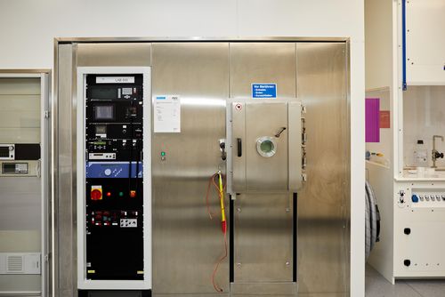
The Balzers PLS 570 is used to deposit thin metallic layers using thermal and electron beam evaporators. In one deposition run in a high-vacuum environment, it is possible to deposit material on up to four 4 inch wafers. Film thickness ranges from a few nanometers to micrometers and the growth rates are monitored using an oscillating crystal. Available materials are: Cr, Al, Au, Ge, Ti, Pd, Pt, Ag, Si, Ni, C, AuSb, AlSi, Mo.
Contact person: Thomas Fromherz
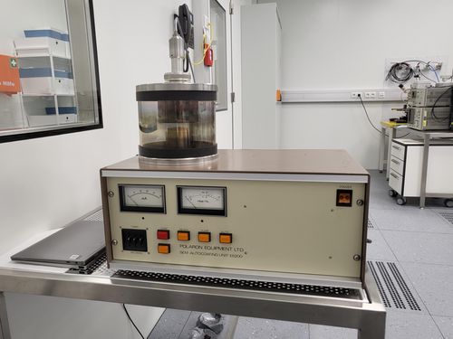
The system is dedicated to sample preparation (thin metal coating) for non-conducting specimens for scanning electron microscopy.
Contact person: Thomas Fromherz
The system uses thermal and electron beam evaporators for the deposition of thin layers of insulating materials. In a high-vacuum environment, up to eight 2 inch wafers can be processed simultaneously at substrate temperatures up to 250°C. Typical layer thicknesses range from a few nanometers to micrometers. The growth rates are measured using an oscillating crystal. Available materials: Al2O3, SiO2, TiO2, ITO, Ta2O5, HfO2
Contact person: Thomas Fromherz
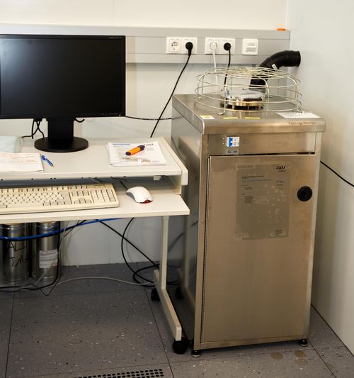
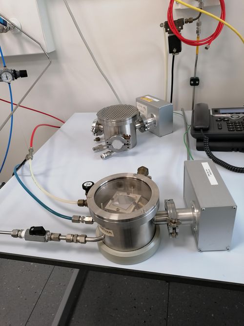
The Savannah 100 Atomic Layer Deposition (ALD) system is used for the deposition of thin layers on flat substrates with diameters up to 100 mm. A wide variety of materials (Alumina, Hafnia, Titania) can be deposited. The method is particularly suited for a conformal coating of three-dimensional structures.
Contact person: Armando Rastelli
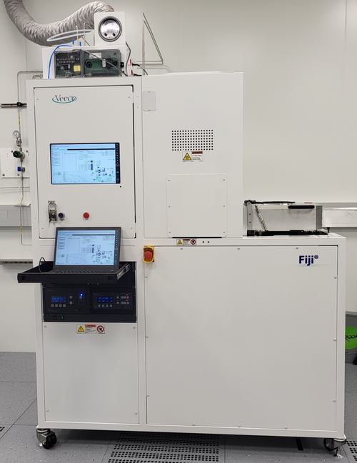
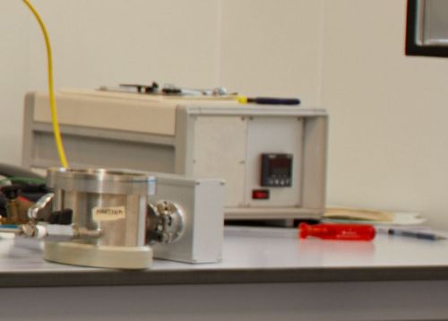
The Fiji G2 Plasma-Enhanced Atomic Layer Deposition (PEALD) system is used for the deposition of thin layers on epi-ready substrates with diameters up to 200 mm. The system can accommodate up to 6 precursors, being mainly employed for the growth of nitrides (NbN, TiN, AlN, MoN). In addition, this system can be used for the deposition of other materials like functional oxides.
Contact Persons: Alberta Bonanni, Rajdeep Adhikari, Bogdan Faina
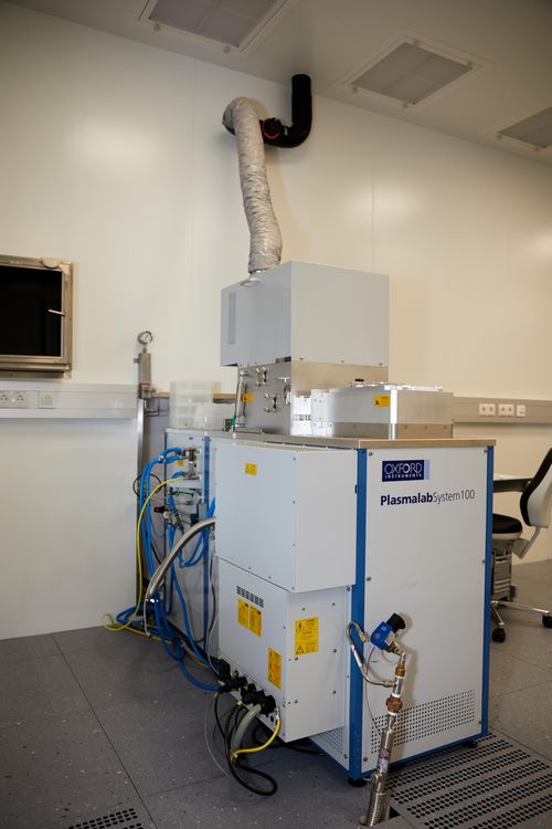
The Oxford PlasmaLab 80 plus system uses SiH4, NH3, and N2O for the deposition of thin SiO2 and Si3N4 layers, e.g., for the fabrication of Bragg mirrors. During deposition, the substrates with sizes up to 100 mm in diameter can be heated up to 750°C.
Contact person: Moritz Brehm
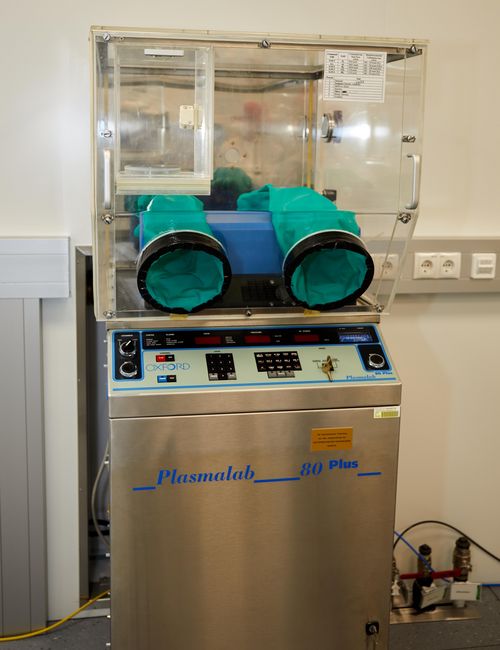
The system can be used to etch samples of Group-IV material in a Bosch process up to 500 µm deep. For such a process, etching steps and surface passivation steps alternate. In the cryo process, performed at temperatures down to -150°C, etching depths of a few nanometers and defined sidewall inclination angles can be precisely obtained. Used gases are He, Ar, C4F8, CHF3, SF6, CF4, O2
Contact person: Moritz Brehm
The system, currently being acquired, equipped with Ar, BCl3, Cl2, O2 and SF6 , will be employed for the etching of photonic structures in arsenides and nitrides.
A large variety of chemicals is employed for selective, isotropic, and anisotropic etching of various insulating, semiconducting and metallic layers.
The following materials can be etched in this system: SF6, CF4, O2, Ar, H2, Si, SiGe, SiNx, SiOx
Contact persons: Stephan Bräuer, Thomas Fromherz
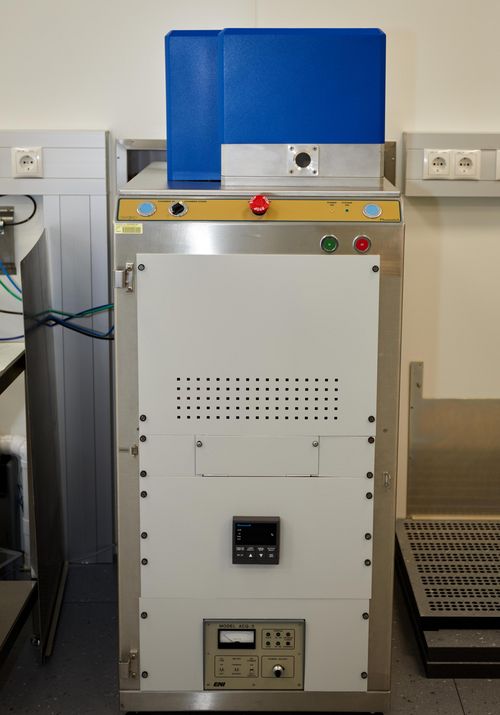
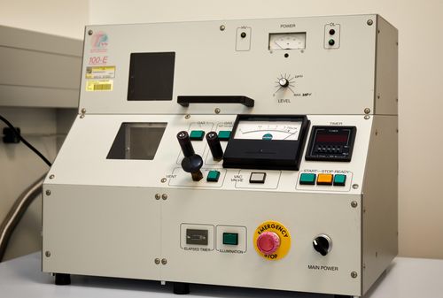
The TePla 100-E asher is a plasma system for sample cleaning and, in particular, for the removal of remains of photoresist. An O2 plasma obtained at powers from 100 W to 250 W is employed to clean substrates with sizes up to 100 mm.
Contact person: Thomas Fromherz
The Die Bonder is mostly used for the integration of III-V semiconductor structures on top of piezoelectric actuators to achieve strain-tunable quantum devices. Currently Au thermocompression bonding and SU8 bonding are used.
Contact Person: Armando Rastelli (Tobias Krieger und Barbara Lehner)
The Kulicke and Soffa Model 4526 is a wedge wire bonder that can be operated using aluminum and gold wires in automatic or manual mode to make electric contact between the fabricated semiconductor devices and chip carriers.
Contact Person: Armando Rastelli
The system is used to study the surface topography and structure morphology after lithographic, etching, and deposition procedures with nanometer precision.
Contact person: Gunther Springholz
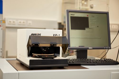
The profilometer Ambios XP1 can be used to determine etch-depths and surface topography through line profiles.
Contact person: Gunther Springholz
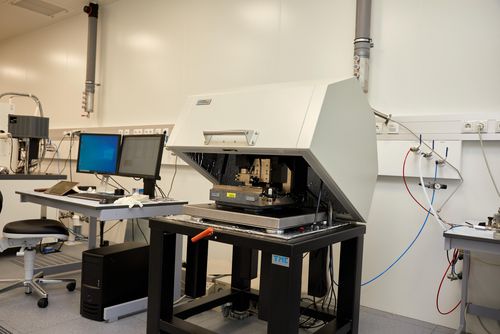
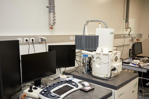
The system is used to characterize samples with nanometer resolution. Top-view images and pictures from tilted images can be recorded using an electron beam with energies up to 30 keV.
Contact person: Alma Halilovic
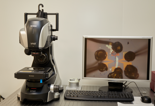
The Keyence VHX-7000 digital microscope offers a high magnification and accuracy with a wide array of functions and features. It can be used for both 2D and 3D measurements. Operations like alignment and focus adjustment is fully automatic. Features such as ‘Optical Shadow Effect Mode’ make subtle contours stand out (in colour) and enhance uneven surfaces and stains. Observations using the fully integrated head can be carried outautomatically at magnifications from 20x to 6000x without manually changing the lens.
Contact persons: Alberta Bonanni (Katharina Burgholzer, Soma Adhikari)
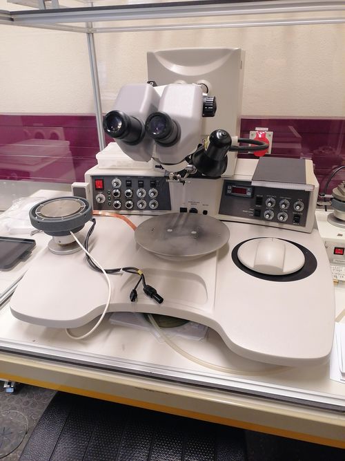
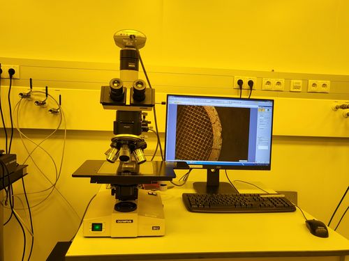
The Olympus BH-2 is an optical microscope used to investigate samples and devices. Magnifications of 5x, 20x, 50x, and 100x can be selected, and the samples can be characterized (structure sizes, defects etc.) using dedicated software.
Contact person: Thomas Fromherz
Two annealing ovens can be used for thermal treatment at various temperatures of Group-IV devices. Annealing gases, such as N2 and Varigon H5 can be used.
Contact person: Thomas Fromherz
The annealing oven that can be used for thermal treatment at various temperatures of Group-III-V devices. Annealing gases, such as N2 and Varigon H5 can be used.
Contact person: Armando Rastelli
The rapid thermal annealer is used to oxidize semiconductor samples with sizes of up to four inches in diameter. The annealer can be operated at temperatures up to 1200°C and under O2 and N2 atmosphere.
Contact person: Armando Rastelli
Johannes Kepler University Linz
Altenberger Straße 69
4040 Linz, Austria
 Go to JKU Homepage
