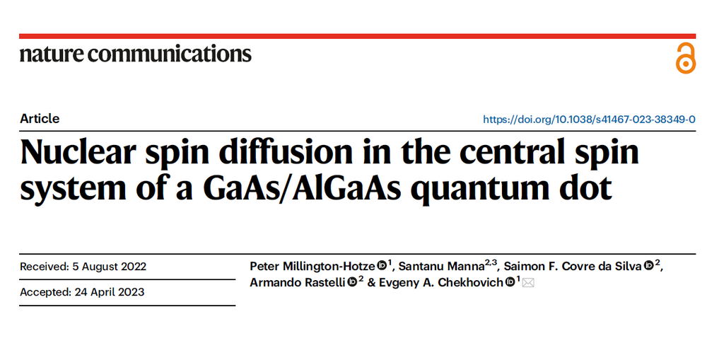
The spin diffusion concept provides a classical description of a purely quantum-mechanical evolution in inhomogeneously polarized many-body systems such as nuclear spin lattices. The central spin of a localized electron alters nuclear spin diffusion in a way that is still poorly understood. Here, spin diffusion in a single GaAs/AlGaAs quantum dot is witnessed in the most direct manner from oscillatory spin relaxation dynamics. Electron spin is found to accelerate nuclear spin relaxation, from which we conclude that the long-discussed concept of a Knight-field-gradient diffusion barrier does not apply to GaAs epitaxial quantum dots. Our experiments distinguish between non-diffusion relaxation and spin diffusion, allowing us to conclude that diffusion is accelerated by the central electron spin. Such acceleration is observed up to unexpectedly high magnetic fields – we propose electron spin-flip fluctuations as an explanation. Diffusion-limited nuclear spin lifetimes range between 1 and 10 s, which is sufficiently long for quantum information storage and processing.
*********************************************************************************************************************************************************************************************************************************************************************************************
L. Zaporski, N. Shofer, J. H. Bodey, S. Manna, G. Gillard, M. Hayhurst Appel, C. Schimpf, S. F. Covre da Silva, J. Jarman, G. Delamare, G. Park, U. Häusler, E. A. Chekhovich, A. Rastelli, D. A. Gangloff, M. Atatüre, C. Le Gall
 © Leon Zaporski, University of Cambridge
Combining highly coherent spin control with efficient light-matter coupling offers great opportunities for quantum communication and computing. Optically active semiconductor quantum dots have unparalleled photonic properties but also modest spin coherence limited by their resident nuclei. The nuclear inhomogeneity has thus far bound all dynamical decoupling measurements to a few microseconds. Here, we eliminate this inhomogeneity using lattice-matched GaAs–AlGaAs quantum dot devices and demonstrate dynamical decoupling of the electron spin qubit beyond 0.113(3) ms. Leveraging the 99.30(5)% visibility of our optical π-pulse gates, we use up to Nπ = 81 decoupling pulses and find a coherence time scaling of N0.75(2)π. This scaling manifests an ideal refocusing of strong interactions between the electron and the nuclear spin ensemble, free of extrinsic noise, which holds the promise of lifetime-limited spin coherence. Our findings demonstrate that the most punishing material science challenge for such quantum dot devices has a remedy and constitute the basis for highly coherent spin–photon interfaces.
*********************************************************************************************************************************************************************************************************************************************************************************************
B. U. Lehner, T. Seidelmann, G. Undeutsch, C.Schimpf, S. Manna, M. Gawelczyk, S. F. Covre da Silva, X. Yuan, S. Stroj, D. E. Reiter,V. M. Axt, A. Rastelli
 ©Barbara Lehner
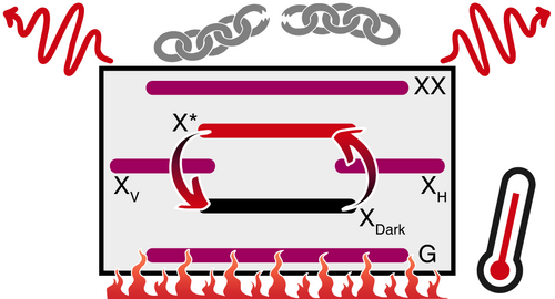
Entangled photon pairs are essential for a multitude of quantum photonic applications. To date, the best performing solid-state quantum emitters of entangled photons are semiconductor quantum dots operated around liquid-helium temperatures. To favor the widespread deployment of these sources, it is important to explore and understand their behavior at temperatures accessible with compact Stirling coolers. Here we study the polarization entanglement among photon pairs from the biexciton–exciton cascade in GaAs quantum dots at temperatures up to ∼65 K. We observe entanglement degradation accompanied by changes in decay dynamics, which we ascribe to thermal population and depopulation of hot and dark states in addition to the four levels relevant for photon pair generation. Detailed calculations considering the presence and characteristics of the additional states and phonon-assisted transitions support the interpretation. We expect these results to guide the optimization of quantum dots as sources of highly entangled photons at elevated temperatures.
*********************************************************************************************************************************************************************************************************************************************************************************************
The following article has been selected for the cover page of Advanced Photonics Vol. 3, Issue 6 (2021):
C. Schimpf, S. Manna, S. Filipe Covre da Silva, M. Aigner, A. Rastelli
Entanglement-based quantum key distribution with a blinking-free quantum dot operated at a temperature up to 20 K, opens an external URL in a new window
Advanced Photonics 3(6), 065001 (17 December 2021).
C. Schimpf, M. Reindl, D. Huber, B. Lehner, S. Filipe Covre da Silva, S. Manna, M. Vyvlecka, P. Walther, A. Rastelli
Quantum cryptography with highly entangled photons from semiconductor quantum dots, opens an external URL in a new window
Sci. Adv. 7, eabe8905 (2021).
************************************************************************************************************
The cover design, opens an external URL in a new window of the article Bright Single Photon Emission from Quantum Dots Embedded in a Broadband Planar Optical Antenna, opens an external URL in a new window by H. Huang, S. Manna, C. Schimpf, M. Reindl, X. Yuan, Y. Zhang, S. Covre da Silva and A. Rastelli (Adv. Optical Mater. 2001490, 2021) has been featured on the inside cover of the issue of "Advanced Optical Materials" 7, 2021.
Abstract:
A planar metal–oxide–semiconductor structure, capable of beaming the photons emitted by epitaxial quantum dots into free space, has been designed and implemented by Huying Huang, Santanu Manna, Armando Rastelli and co‐workers (see article number 2001490, opens an external URL in a new window). The structure is tolerant to fabrication imperfections and allows the photon outcoupling efficiency to be greatly enhanced without any deterministic positioning of the quantum emitters.
************************************************************************************************************
F. Basso Basset, F. Salusti, L. Schweickert, M. Rota, D. Tedeschi, S. Filipe Covre da Silva, E. Roccia, V. Zwiller, K. Jöns, A. Rastelli, R. Trotta
Quantum teleportation with imperfect quantum dots, opens an external URL in a new window
npj Quantum Information 7 (2021)
************************************************************************************************************
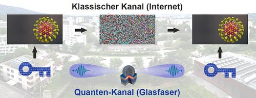
E. A. Chekhovich, S. Filipe Covre da Silva, A. Rastelli
Nature Nanotechnology 15, 999-1004 (2020).
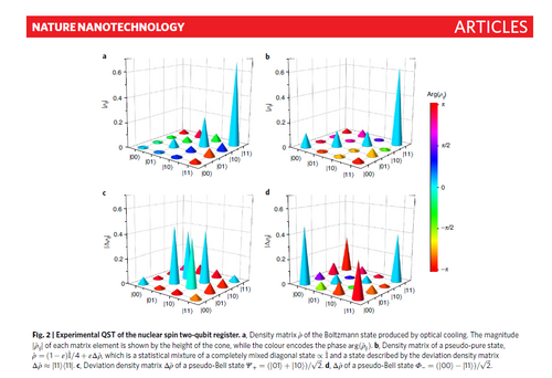
Epitaxial quantum dots (QDs) have long been identified as promising charge spin qubits offering an efficient interface to quantum light and advanced semiconductor nanofabrication technologies. However, charge spin coherence is limited by interaction with the nanoscale ensemble of atomic nuclear spins, which is particularly problematic in strained self-assembled dots. Here, we use strain-free GaAs/AlGaAs QDs, demonstrating a fully functioning two-qubit quantum register using the nanoscale ensemble of arsenic quadrupolar nuclear spins as its hardware. Tailored radio-frequency pulses allow quantum state storage for up to 20 ms, and are used for few-microsecond single-qubit and two-qubit control gates with fidelities exceeding 97%. Combining long coherence and high-fidelity control with optical initialization and readout, we implement benchmark quantum computations such as Grover’s search and the Deutsch–Jozsa algorithm. Our results identify QD nuclei as a potential quantum information resource, which can complement charge spins and light particles in future QD circuits.
************************************************************************************************************
Elham M. T. Fadaly, Alain Dijkstra, Jens René Suckert, Dorian Ziss, Marvin A. J. van Tilburg, Chenyang Mao, Yizhen Ren, Victor T. van Lange, Ksenia Korzun, Sebastian Kölling, Marcel A. Verheijen, David Busse, Claudia Rödl, Jürgen Furthmüller, Friedhelm Bechstedt, Julian Stangl, Jonathan J. Finley, Silvana Botti, Jos E. M. Haverkort, Erik P. A. M. Bakkers.
Emitting light from silicon has been the ‘Holy Grail’ in the microelectronics industry for decades. Solving this puzzle would revolutionize computing, as chips will become faster than ever. A multi-national research group lead by scientists from Eindhoven University of Technology and with contributions from JKU Linz now succeeded: they have developed an alloy with silicon that can emit light. The results have been published in the journal Nature.
Every year we use and produce significantly more data. But our current technology, based on electronic chips, is reaching its ceiling. The limiting factor is heat, resulting from the resistance that the electrons experience when traveling through the copper lines connecting the many transistors on a chip. If we want to continue transferring more and more data every year, we need a new technique that does not produce heat. Bring in photonics, which uses photons (light particles) to transfer data.In contrast to electrons, photons do not experience resistance. As they have no mass or charge, they will scatter less within the material they travel through, and therefore no heat is produced. The energy consumption will therefore be reduced. Moreover, by replacing electrical communication within a chip by optical communication, the speed of on-chip and chip-to-chip communication can be increased by a factor 1000. Data centers would benefit most, with faster data transfer and less energy usage for their cooling system. But these photonic chips will also bring new applications within reach. Think of laser-based radar for self-driving cars and chemical sensors for medical diagnosis or for measuring air and food quality.To use light in chips, you will need a light source; an integrated laser. The main semiconductor material that computer chips are made of is silicon. But bulk silicon is extremely inefficient at emitting light, and so was long thought to play no role in photonics. Thus, scientists turned to more complex semiconductors, such as gallium arsenide and indium phosphide. These are good at emitting light but are more expensive than silicon and are hard to integrate into existing silicon microchips.To create an all-silicon laser, scientists needed to produce a form of silicon that can emit light. That’s exactly what researchers from Eindhoven University of Technology now succeeded in. Together with researchers from the universities of Jena, JKU Linz and Munich, they combined silicon and germanium in a hexagonal structure that is able to emit light. A breakthrough after 50 years of work.
The work received major response from the international scientific-press:
15.04.2020 - Light-emitting hexagonal SiGe promises integrated photonics breakthroughy, opens an external URL in a new window; (optics.org)
10.04.2020 - Direct-bandgap emission achieved from hexagonal Ge and SiGe alloys, opens an external URL in a new window; (semiconductor-today.com)
09.04.2020 - Light-emitting SiGe alloys developed, opens an external URL in a new window; (electronicsweekly.com)
09.04.2020 - SiGe alloys usable in silicon photonics emit light via direct bandgap, opens an external URL in a new window; (laserfocusworld.com)
09.04.2020 - Durchbruch für Photonik-Chips, opens an external URL in a new window; (pro-physik.de)
08.04.2020 - Nanostructured alloys light the way to silicon-based photonics, opens an external URL in a new window; (nature.com)
08.04.2020 - Silicon-based light emitter is ‘Holy Grail’ of microelectronics, say researchers, opens an external URL in a new window; (physicsworld.com)
*********************************************************************************************************************************************************************************************************************************************************************************************
E. D. L. Rienks, S. Wimmer, J. Sanchez-Barriga, O. Caha, P. S. Mandal, J. Ruzicka, A. Ney, H. Steiner, V. Volobuiev, H. Groiss, M. Albu, G. Kothleitner, J. Michalicka, S. A. Khan, J. Minar, H. Ebert, G. Bauer, F. Freyse, A.Varykhalov, O. Rader, G. Springholz
Magnetically doped topological insulators enable the quantum anomalous Hall effect (QAHE), which provides quantized edge states for lossless charge-transport applications. The edge states are hosted by a magnetic energy gap at the Dirac point, but hitherto all attempts to observe this gap directly have been unsuccessful. Observing the gap is considered to be essential to overcoming the limitations of the QAHE, which so far occurs only at temperatures that are one to two orders of
magnitude below the ferromagnetic Curie temperature, TC. Here we use lowtemperature photoelectron spectroscopy to unambiguously reveal the magnetic gap of Mn-doped Bi2Te3, which displays ferromagnetic out-of-plane spin texture and opens up only below TC. Surprisingly, our analysis reveals large gap sizes at 1 kelvin of up to 90 millielectronvolts, which is five times larger than theoretically predicted. Using multiscale analysis we show that this enhancement is due to a remarkable structure modification induced by Mn doping: instead of a disordered impurity system, a self-organized alternating sequence of MnBi2Te4 septuple and Bi2Te3 quintuple layers is formed. This enhances the wavefunction overlap and size of the magnetic gap. Mn-doped Bi2Se3 and Mn-doped Sb2Te3 form similar heterostructures, but for Bi2Se3 only a nonmagnetic gap is formed and the magnetization is in the surface plane. This is explained by the smaller spin–orbit interaction by comparison with Mn-doped Bi2Te3. Our findings provide insights that will be crucial in pushing lossless transport in topological insulators towards roomtemperature applications.
*********************************************************************************************************************************************************************************************************************************************************************************************
Massimo Gurioli, Zhiming Wang, Armando Rastelli, Takashi Kuroda, Stefano Sanguinetti
The long dreamed ‘quantum internet’ would consist of a network of quantum nodes (solid-state or atomic systems) linked by flying qubits, naturally based on photons, travelling over long distances at the speed of light, with negligible decoherence. A key component is a light source, able to provide single or entangled photon pairs. Among the different platforms, semiconductor quantum dots (QDs) are very attractive, as they can be integrated with other photonic and electronic components in miniaturized chips. In the early 1990s two approaches were developed to synthetize self-assembled epitaxial semiconductor QDs, or ‘artificial atoms’—namely, the Stranski–Krastanov (SK) and the droplet epitaxy (DE) methods. Because of its robustness and simplicity, the SK method became the workhorse to achieve several breakthroughs in both fundamental and technological areas. The need for specific emission wavelengths or structural and optical properties has nevertheless motivated further research on the DE method and its more recent development, local droplet etching (LDE), as complementary routes to obtain high-quality semiconductor nanostructures. The recent reports on the generation of highly entangled photon pairs, combined with good photon indistinguishability, suggest that DE and LDE QDs may complement (and sometimes even outperform) conventional SK InGaAs QDs as quantum emitters. We present here a critical survey of the state of the art of DE and LDE, highlighting the advantages and weaknesses, the achievements and challenges that are still open, in view of applications in quantum communication and technology.
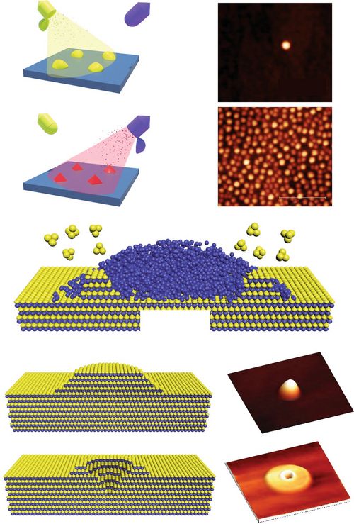 Fig. 1 | Droplet epitaxy. a, Droplet epitaxy schematics: in a molecular beam epitaxy chamber, group-III metals are deposited at first on the surface
(upper panel), leading to the formation of droplets. After this step (lower panel), the metal source is closed, and group-V flux is supplied to the surface
to crystallize the droplets into 3D nanostructures. b, Examples of high-density (n = 3 × 103 μm–2) and low-density (n = 4 μm–2) QDs obtained on
AlGaAs(001) substrates by varying the substrate temperature between 150 °C and 350 °C during metal deposition. c, Schematics of the DE QD growth
mechanism during group-V (typically As) supply. Process 1 (red arrows): as direct incorporation in the metallic droplet gives rise to GaAs crystallization
at the liquid–solid interface, starting from the triple line. Process 2 (blue arrows): owing to As adsorption on the surface surrounding the droplet, surface
termination is changed and diffusion of Ga out of the droplet by capillary forces takes place. Coming from the droplets edge, Ga atoms can migrate,
covering a mean diffusion length before being incorporated into the GaAs crystal. Blue dots indicate Ga atoms. As atoms are indicated by yellow dots.
d, Atomic force microscopy image (right) and atomistic scheme (left) of a DE QD (top) and a hollow DE nanostructure (bottom). The DE QD was
obtained by crystallizing the droplet at T = 200 °C and As flux ≈ 10–5 torr, thus favouring As direct incorporation into the droplet during the crystallization
step. The hollow nanostructure was obtained by crystallizing the droplet at T = 350 °C and As flux ≈ 10–7 torr on (001) substrates, where process 2
(out-diffusion of metal from the droplet and incorporation in to the bulk) dominates.
Fig. 1 | Droplet epitaxy. a, Droplet epitaxy schematics: in a molecular beam epitaxy chamber, group-III metals are deposited at first on the surface
(upper panel), leading to the formation of droplets. After this step (lower panel), the metal source is closed, and group-V flux is supplied to the surface
to crystallize the droplets into 3D nanostructures. b, Examples of high-density (n = 3 × 103 μm–2) and low-density (n = 4 μm–2) QDs obtained on
AlGaAs(001) substrates by varying the substrate temperature between 150 °C and 350 °C during metal deposition. c, Schematics of the DE QD growth
mechanism during group-V (typically As) supply. Process 1 (red arrows): as direct incorporation in the metallic droplet gives rise to GaAs crystallization
at the liquid–solid interface, starting from the triple line. Process 2 (blue arrows): owing to As adsorption on the surface surrounding the droplet, surface
termination is changed and diffusion of Ga out of the droplet by capillary forces takes place. Coming from the droplets edge, Ga atoms can migrate,
covering a mean diffusion length before being incorporated into the GaAs crystal. Blue dots indicate Ga atoms. As atoms are indicated by yellow dots.
d, Atomic force microscopy image (right) and atomistic scheme (left) of a DE QD (top) and a hollow DE nanostructure (bottom). The DE QD was
obtained by crystallizing the droplet at T = 200 °C and As flux ≈ 10–5 torr, thus favouring As direct incorporation into the droplet during the crystallization
step. The hollow nanostructure was obtained by crystallizing the droplet at T = 350 °C and As flux ≈ 10–7 torr on (001) substrates, where process 2
(out-diffusion of metal from the droplet and incorporation in to the bulk) dominates.
*********************************************************************************************************************************************************************************************************************************************************************************************
F. Hackl, M. Grydlik, Petr Klenovský, F. Schäffler, T. Fromherz, M. Brehm
Different recombination paths can strongly influence the optical properties of quantum dots. The green, red, and blue surfaces indicate the probability densities of heavy‐hole, Δz, and Δxy electron wave‐functions, respectively, as discussed in article number 1800259, opens an external URL in a new window by Florian Hackl, Thomas Fromherz, Moritz Brehm, and co‐workers.
*********************************************************************************************************************************************************************************************************************************************************************************************
J.Liu, R. Su, Y. Wei, B. Yao, S. F. Covre da Silva, Y. Yu, J. Iles-Smith, K. Srinivasan, A. Rastelli, J. Li, X. Wang
 ©Toan T. Tran
*********************************************************************************************************************************************************************************************************************************************************************************************
Florian Hackl, Martyna Grydlik, Petr Klenovský, Friedrich Schäffler, Thomas Fromherz, Moritz Brehm
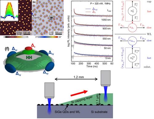
We have identified different recombination paths in Ge/Si quantum dots that contribute significantly to luminescence line broadening in these structures. Using time-resolved spectroscopy, we highlight that the various carrier transition paths are differently influenced by non-radiative carrier recombination such as e.g. Auger-recombination.
*********************************************************************************************************************************************************************************************************************************************************************************************
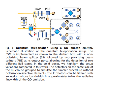
M. Reindl, D. Huber, C. Schimpf, S. F. Covre da Silva, M. B. Rota, H. Huang, V. Zwiller, K. D. Jöns, A. Rastelli, R. Trotta:
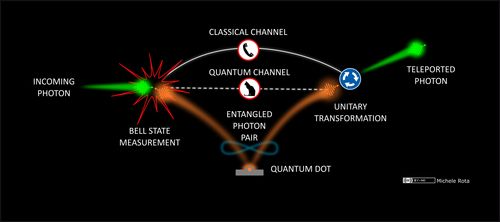
All-optical quantum teleportation lies at the heart of quantum communication science and technology. This quantum phenomenon is built up around the nonlocal properties of entangled states of light that, in the perspective of real-life applications, should be encoded on photon pairs generated on demand. Despite recent advances, however, the exploitation of deterministic quantum light sources in push-button quantum teleportation schemes remains a major open challenge. Here, we perform an important step toward this goal and show that photon pairs generated on demand by a GaAs quantum dot can be used to implement a teleportation protocol whose fidelity violates the classical limit (by more than 5 SDs) for arbitrary input states. Moreover, we develop a theoretical framework that matches the experimental observations and that defines the degree of entanglement and indistinguishability needed to overcome the classical limit independently of the input state. Our results emphasize that on-demand solid-state quantum emitters are one of the most promising candidates to realize deterministic quantum teleportation in practical quantum networks.
*********************************************************************************************************************************************************************************************************************************************************************************************
Xueyong Yuan, Fritz Weyhausen-Brinkmann, Javier Martín-Sánchez, Giovanni Piredda, Vlastimil Křápek, Yongheng Huo, Huiying Huang, Christian Schimpf, Oliver G. Schmidt, Johannes Edlinger, Gabriel Bester, Rinaldo Trotta, Armando Rastelli
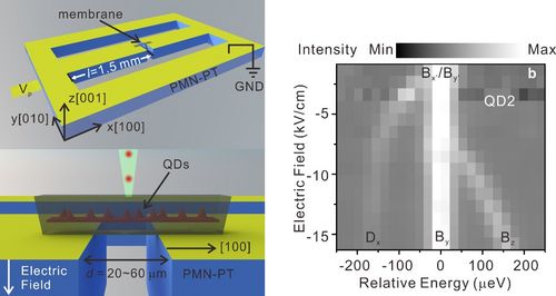 By using a novel piezoelectric actuator featuring geometric strain amplification, we have demonstrated that the natural quantization axis of strain-free GaAs quantum dots can be flipped to lie in the growth plane via moderate uniaxial stress. Together with the computational results, our work illustrate that uniaxial stress could be the right method to obtain quantum-light sources with ideally oriented transition dipoles and enhanced oscillator strengths for integrated quantum photonics.
*********************************************************************************************************************************************************************************************************************************************************************************************
Daniel Huber, Marcus Reindl, Saimon Filipe Covre da Silva, Christian Schimpf, Javier Martín-Sánchez, Huiying Huang, Giovanni Piredda, Johannes Edlinger, Armando Rastelli, and Rinaldo Trotta:
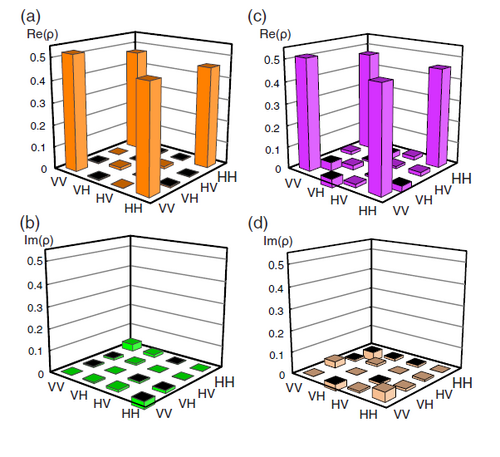
Entangled photon pairs are a key resource for quantum communication. We have now achieved the highest degree of polarization entanglement for photon pairs emitted by quantum dots by combining: 1) High-quality GaAs quantum dots grown by molecular beam epitaxy at our institute and embedded in planar cavities for enhanced light extraction, 2) resonant two-photon excitation for on demand operation, and 3) micro-structured piezoelectric actuators for removing the effect of residual anisotropy in the quantum dot potential. This work shows that quantum dots have the potential to fulfill the criteria of a perfect entangled-photon source.
*********************************************************************************************************************************************************************************************************************************************************************************************
J. Krempaský, S. Muff, J. Minár, N. Pilet, M. Fanciulli, A. P. Weber, E. B. Guedes, M. Caputo, E. Müller, V. V. Volobuev, M. Gmitra, C. A. F. Vaz, V. Scagnoli, G. Springholz, and J. H. Dil:
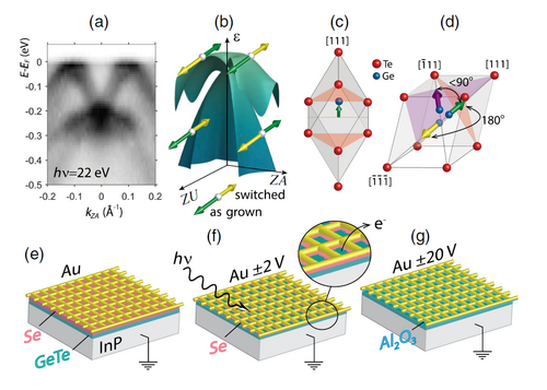
The control of the electron spin by external means is a key issue for spintronic devices. Using spin- and angle-resolved photoemission spectroscopy (SARPES) with three-dimensional spin detection, we demonstrate operando electrostatic spin manipulation in ferroelectric α−GeTe and multiferroic Ge1−xMnxTe. We demonstrate for the first time electrostatic spin manipulation in Rashba semiconductors due to ferroelectric polarization reversal. In multiferroic Ge1−xMnxTe operando SARPES reveals switching of the perpendicular spin component due to electric-field-induced magnetization reversal. This provides firm evidence of magnetoelectric coupling which opens up functionality with a multitude of spin-switching paths in which the magnetic and electric order parameters are coupled through ferroelastic relaxation paths. This work thus provides a new type of magnetoelectric switching intertwined with Rashba-Zeeman splitting in a multiferroic system.
*********************************************************************************************************************************************************************************************************************************************************************************************
A. B. Henriques, X. Gratens, P. A. Usachev, V. A. Chitta, and G. Springholz:
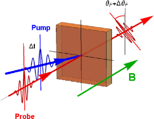 Figure: Scheme of the setup for measuring the time-resolved photoinduced Faraday rotation angle. The linearly polarized probe pulse arrives at the sample when a time Δt has elapsed after the arrival of the pump pulse. We measured ΔθF, the increment in the Faraday rotation of the probe, induced by the pump illumination.
We demonstrate that light resonant with the band gap forces the antiferromagnetic semiconductor EuSe to enter ferromagnetic alignment in the picosecond timescale. A photon generates an electron-hole pair, whose electron forms a supergiant spin polaron of magnetic moment of nearly 6000 Bohr magnetons. By increasing the light intensity, the whole of the illuminated region can be fully magnetized. The key to the novel large photoinduced magnetization mechanism is the huge enhancement of the magnetic susceptibility when both antiferromagnetic and ferromagnetic interactions are present in the material and are of nearly equal magnitude, as is the case in EuSe.
*********************************************************************************************************************************************************************************************************************************************************************************************
B. Mandl, M. Keplinger, M. E. Messing, D. Kriegner, R. Wallenberg, L. Samuelson, G. Bauer, J. Stangl, V. Holy, K. Deppert:
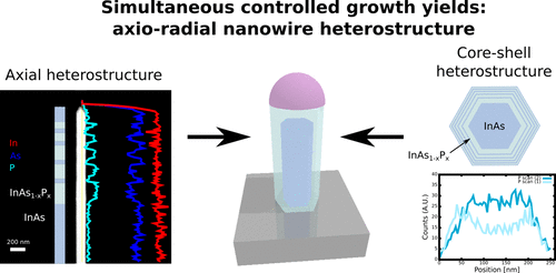
Semiconductors are essential for modern electronic and optoelectronic devices. To further advance the functionality of such devices, the ability to fabricate increasingly complex semiconductor nanostructures is of utmost importance. Nanowires offer excellent opportunities for new device concepts; heterostructures have been grown in either the radial or axial direction of the core nanowire but never along both directions at the same time. This is a consequence of the common use of a foreign metal seed particle with fixed size for nanowire heterostructure growth. In this work, we present for the first time a growth method to control heterostructure growth in both the axial and the radial directions simultaneously while maintaining an untapered self-seeded growth. This is demonstrated for the InAs/InAs1–xPx material system. We show how the dimensions and composition of such axio-radial nanowire heterostructures can be designed including the formation of a “pseudo-superlattice” consisting of five separate InAs1–xPx segments with varying length. The growth of axio-radial nanowire heterostructures offers an exciting platform for novel nanowire structures applicable for fundamental studies as well as nanowire devices. The growth concept for axio-radial nanowire heterostructures is expected to be fully compatible with Si substrates.
*********************************************************************************************************************************************************************************************************************************************************************************************
L. Schweickert, K. D. Jöns, K. D. Zeuner, S. F. Covre da Silva, H. Huang, T. Lettner, M. Reindl, J. Zichi, R. Trotta, A. Rastelli, V. Zwiller:
Our collaborators at KTH Stockholm demonstrated an unprecedented single photon purity in the solid-state which exceeds the performance of any available single photon source to date. The used quantum dot source was grown in Linz.
*********************************************************************************************************************************************************************************************************************************************************************************************
V. Volobuiev, P. S. Mandal, M. Galicka, O. Caha, J. Sanchez-Barriga, D. Di Sante, A. Varykhalov, A. Khiar, S. Picozzi, G. Bauer, P. Kacman, R. Buczko, O. Rader, G. Springholz:
The topological properties of lead‐tin chalcogenide topological crystalline insulators can be widely tuned by temperature and composition. It is shown that bulk Bi doping of epitaxial Pb1‐xSnxTe (111) films induces a giant Rashba splitting at the surface that can be tuned by the doping level. Tight binding calculations identify their origin as Fermi level pinning by trap states at the surface.
*********************************************************************************************************************************************************************************************************************************************************************************************
The article "Photoluminescence enhancement through vertical stacking of defect-engineered Ge on Si quantum dots", by H. Groiss, L. Spindlberger, P. Oberhumer, F. Schäffler, T. Fromherz, M. Grydlik and M. Brehm,
has been chosen for the 2017 Semiconductor Science and Technology (SST) highlight collection.
 Image: Groiss et al. 2017 Semicond. Sci. Technol. 32 02LT01
*********************************************************************************************************************************************************************************************************************************************************************************************
The topical review "Site-controlled and advanced epitaxial Ge/Si quantum dots: fabrication, properties and applications" by Moritz Brehm and Martyna Grydlik / was included in the Highlights of Nanotechnology 2017, opens an external URL in a new window.
This collection includes outstanding articles and Topical Reviews published in the journal during 2017. These articles were selected on the basis of a range of criteria including referee endorsements, presentation of outstanding research and popularity with our online readership. The articles will be free to read until the end of December 2018. Our article is open access anyways, thanks to Funding from the FWF.
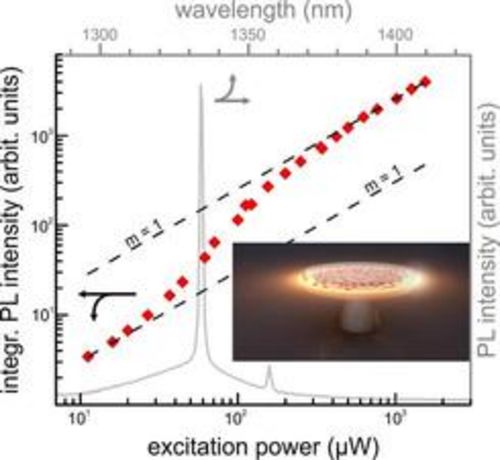 Image: Moritz Brehm and Martyna Grydlik 2017 Nanotechnology 28 392001
*********************************************************************************************************************************************************************************************************************************************************************************************
P. S. Mandal, G. Springholz, V. V. Volobuev, O. Caha, A. Varykhalov, E. Golias, G. Bauer, O. Rader, J. Sánchez-Barriga:
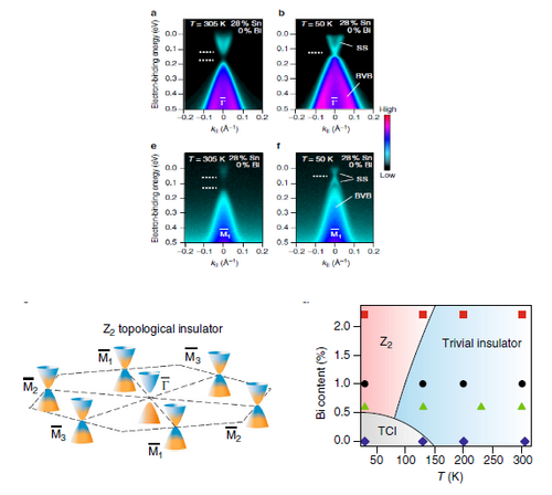
Topological insulators constitute a new phase of matter protected by symmetries. Time-reversal symmetry protects strong topological insulators of the Z2 class, which possess an odd number of metallic surface states with dispersion of a Dirac cone. Topological crystalline insulators are merely protected by individual crystal symmetries and exist for an even number of Dirac cones. Here, we demonstrate that Bi-doping of Pb1−xSnxSe (111) epilayers induces a quantum phase transition from a topological crystalline insulator to a Z2 topological insulator.
*********************************************************************************************************************************************************************************************************************************************************************************************
B. A. Assaf, T. Phuphachong, E. Kampert, V. Volobuiev, P. S. Mandal, J. Sanchez-Barriga, O. Rader, G. Bauer, G. Springholz, L. A. de Vaulchier, Y. Guldner:
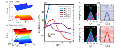
Negative longitudinal magnetoresistance (NLMR) is shown to occur in topological materials in the extreme quantum limit, when a magnetic field is applied parallel to the excitation current. We perform pulsed and dc field measurements on Pb1−xSnxSe epilayers where the topological state can be chemically tuned. The NLMR is observed in the topological state, but is suppressed and becomes positive when the system becomes trivial. In a topological material, the lowest N=0 conduction Landau level disperses down in energy as a function of increasing magnetic field, while the N=0 valence Landau level disperses upwards. This anomalous behavior is shown to be responsible for the observed NLMR. Our work provides an explanation of the outstanding question of NLMR in topological insulators and establishes this effect as a possible hallmark of bulk conduction in topological matter.
*********************************************************************************************************************************************************************************************************************************************************************************************
H. Groiß, M. Glaser, M. Schatzl, M. Brehm, D. Gerthsen, D. Roth, P. Bauer, F. Schäffler
*********************************************************************************************************************************************************************************************************************************************************************************************
M. Schatzl, F. Hackl, M. Glaser, P. Rauter, M. Brehm, L. Spindlberger, A. Simbula, M. Galli, T. Fromherz, F. Schäffler
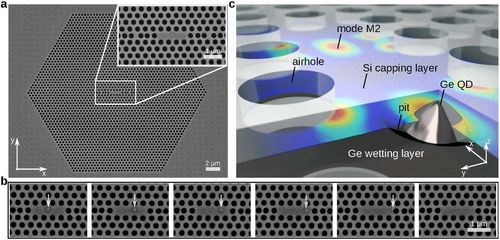 Figure 1. Layout of the single-dot photonic crystal cavities. (a) Scanning electron micrograph of a complete PCR structure with a single Ge QD in
the center of the L3 cavity (inset), fabricated in one growth and processing run. The QD array with twice the period of the PC array remains only
outside the photonic structure. The inset reveals the modifications of the air hole positions adjacent to the cavity of our adapted high-Q design. (b)
Representative set of six simultaneously fabricated L3 cavities in which the Ge QD position (marked by an arrow) was varied along the horizontal
center line of the cavity. As a reference, one of the cavities was fabricated without a pit for QD nucleation; that is, it contained only the Ge wetting
layer (last frame). (c) Schematic view (not to scale) of a single QD positioned in the calculated field energy density maximum of the M2 cavity
mode. The structural components of the single-dot emitter system are indicated. Note that the dot position is determined by the pit in the
prepatterned substrate, as described in the Methods section. The displayed dot shape was modeled on an atomic force micrograph.
Figure 1. Layout of the single-dot photonic crystal cavities. (a) Scanning electron micrograph of a complete PCR structure with a single Ge QD in
the center of the L3 cavity (inset), fabricated in one growth and processing run. The QD array with twice the period of the PC array remains only
outside the photonic structure. The inset reveals the modifications of the air hole positions adjacent to the cavity of our adapted high-Q design. (b)
Representative set of six simultaneously fabricated L3 cavities in which the Ge QD position (marked by an arrow) was varied along the horizontal
center line of the cavity. As a reference, one of the cavities was fabricated without a pit for QD nucleation; that is, it contained only the Ge wetting
layer (last frame). (c) Schematic view (not to scale) of a single QD positioned in the calculated field energy density maximum of the M2 cavity
mode. The structural components of the single-dot emitter system are indicated. Note that the dot position is determined by the pit in the
prepatterned substrate, as described in the Methods section. The displayed dot shape was modeled on an atomic force micrograph.
Johannes Kepler University Linz
Altenberger Straße 69
4040 Linz, Austria
 Go to JKU Homepage
