Dr. Chunguang Hu, Dr. Lidong Sun,
Prof. Dr. Peter Zeppenfeld
We have developed a new type of reflectance difference (RD) spectrometer for fast spectroscopic measurements based on a rotating-compensator (RC) design. The instrument uses a 1024 element Si photodiode linear array for simultaneous multiwavelength detection. High quality RD spectra covering a spectral range from 1.5 to 4.5 eV can be acquired within a few seconds. A detailed description of the working principle, the instrumentation, and the algorithms used for data collection and reduction can be found in Ref. [1], together with a discussion of errors introduced by lamp instability and optical imperfections of the compensator.
For more information please contact:
Lidong Sun or Peter Zeppenfeld
References:
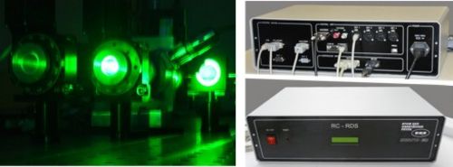 Figure 1
Left Panel: The RCRDS optical components mounted on an optical table. Left panels: Back and front side of the homebuilt RCRDS-controller.
Figure 1
Left Panel: The RCRDS optical components mounted on an optical table. Left panels: Back and front side of the homebuilt RCRDS-controller.
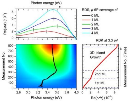 Figure 2
p-6P thin film growth on the Cu(110)-(2x1)O surface at 310 K. The contour map in the lower left is a 2D visualization of all RD spectra (x≅E) as a function of the measurement number (y ≅ t) recorded during film growth. The dots on the image mark the maximum peak intensities derived by fitting polynomials to each RD spectrum. The graph windows at the top and on the right of the 2D image are used to show cuts
along the x and y directions of the central image. The five RD spectra I(E) shown in the upper panel correspond to a nominal film thickness of 0, 1, 2, 3, and 4 ML of p-6P. The lower right panel shows a plot of the RDS signal at a fixed photon energy of 3.3 eV as a function of measurement number (time). The dotted lines mark the three stages of growth that can be identified from the characteristic changes in the slopes of the curve, namely, (i) the start of the evaporation of p-6P after opening the shutter, (ii) the completion of the first monolayer, (iii) the completion of the second monolayer, (iv) and the subsequent 3D island growth until the shutter is closed.
Figure 2
p-6P thin film growth on the Cu(110)-(2x1)O surface at 310 K. The contour map in the lower left is a 2D visualization of all RD spectra (x≅E) as a function of the measurement number (y ≅ t) recorded during film growth. The dots on the image mark the maximum peak intensities derived by fitting polynomials to each RD spectrum. The graph windows at the top and on the right of the 2D image are used to show cuts
along the x and y directions of the central image. The five RD spectra I(E) shown in the upper panel correspond to a nominal film thickness of 0, 1, 2, 3, and 4 ML of p-6P. The lower right panel shows a plot of the RDS signal at a fixed photon energy of 3.3 eV as a function of measurement number (time). The dotted lines mark the three stages of growth that can be identified from the characteristic changes in the slopes of the curve, namely, (i) the start of the evaporation of p-6P after opening the shutter, (ii) the completion of the first monolayer, (iii) the completion of the second monolayer, (iv) and the subsequent 3D island growth until the shutter is closed.
Johannes Kepler University Linz
Altenberger Straße 69
4040 Linz, Austria
 Go to JKU Homepage
